 Шэньчжэньская компания по производству точности Lianjincheng, ООО.
- Телефон: +86-18320991841
- Электронная почта: sales@ljcpcbtech.com
- sales01@ljcpcbtech.com

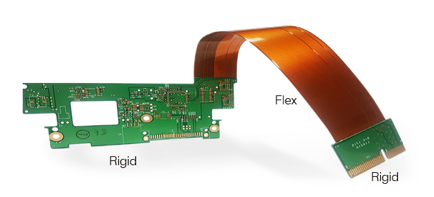
Жестко-гибкая печатная плата
Определение жесткой гибкой печатной платы
A Жесткая гибкая плата - это плата, которая объединяет характеристики гибкой платы (Fpc) и жесткая плата (Pcb). Он объединяет гибкую плату с жесткой платой в соответствии с соответствующими требованиями процесса посредством таких процессов, как нажатие, тем самым формируя плату с характеристиками как FPC, так и PCB. Эта комбинированная плата не только наследует сгибаемость гибкой платы и жесткости жесткой платы, но также имеет преимущества экономии внутреннего пространства продукта и удовлетворения потребностей развития в направлении высокой плотности, миниатюризация, легкий вес, худость, и высокая надежность.
Определение жесткой гибкой печатной платы
Преимущество жесткой гибкой печатной платы
Космическая эффективность: Жесткие гибкие печатные платы чрезвычайно пространственные, потому что они устраняют необходимость в разъемах и снижают необходимость в дополнительных соединениях. Они могут быть сложены или согнуты, чтобы вписаться в узкие места, Сделать их идеальными для компактного и густого расположенного электронного оборудования.
Надежность: Меньше разъемов есть, меньше потенциальных точек отказа, который повышает надежность всей системы. Жесткие гибкие печатные платы менее склонны к проблемам, связанным с разъемом.
Долговечность: Жесткая гибкая пласка может противостоять механическому напряжению, Изменения вибрации и температуры, сделать их подходящими для использования в суровых условиях.
Рентабельный: Жесткая гибкая печатная плата поможет вам минимизировать общий размер печатной платы, Замените разъемы до борта, и уменьшить количество процессов сборки. Это может привести к значительной экономии в затратах на логистику.
Сложная геометрия: Технология жесткой гибки позволяет создавать сложные формы платы и трехмерные конфигурации, которые трудно достичь с помощью традиционных ПХБ.
Обзор возможностей жесткой гибкой печатной платы
| Элемент | Массовое производство | Прототип |
| Количество слоев | 2-18 л | 2-20 л |
| Максимальный размер доски | 480*800мм | 480*800мм |
| Схема размерной толерантности | ± 0,10 мм (≤100 мм) ± 0,10%мм (> 100 мм) |
± 0,10 мм (≤100 мм) ± 0,10%мм (> 100 мм) |
| Диапазон толщины | 0.3-3.2мм | 0.3-4мм |
| Толерантность к толщине (THK≥0,8 мм) | ± 8% | ± 8% |
| Толерантность к толщине (Тур<0.8мм) | ± 10% | ± 8% |
| Диэлектрическая толщина | 0.03-5.00мм | 0.03-5.5мм |
| Минимальная наружная ширина /расстояние между линиями /расстоянием линий | 0.075/0.075мм (Законченная медь) | 0.075/0.075мм (Законченная медь) |
| Мин внутренний слой ширина /расстояние между линиями линий | 0.05мм/0,05 мм (Базовая медь 12ум) | 0.05мм/0,05 мм (Базовая медь 12ум) |
| Через кольцо с подушкой мин (Двусторонний) | ≥0,05 мм | ≥0,05 мм |
| Минимальное расстояние от проводника от контура или npth | ≥0,15 мм | ≥0,15 мм |
| Мин кольцевое кольцо (Четыре слоя и выше) | ≥0,1 мм | ≥0,1 мм |
| Внешняя готовая медь | 35-105один | 35-140один |
| Внутренняя медь | 12-70один | 12-105один |
| Размер отверстия (Механическая тренировка) | 0.10-6.35мм | 0.10-6.5мм |
| Лазерное бурение (Требуется заполнение отверстий) | 0.075-0.1мм | 0.05-0.15мм |
| Апертура терпимость (Механическая тренировка) | ПТГ ± 0,075 мм NPTH ± 0,05 мм | ПТГ ± 0,05 мм NPTH ± 0,04 мм |
| Допустимость в положении отверстия (Механическая тренировка) | ± 0,05 мм | ± 0,05 мм |
| Минимальное расстояние от внутреннего края отверстия до другого сетевого проводника | (4 Слои) 5мил, (6 Слои) 6мил, (8 Слои и выше) 8мил |
(4 Слои) 5мил, (6 Слои) 6мил, (8 Слои и выше) 8мил |
| Отклонение выравнивания между слоями (Не примечательные слои) | ± 0,1 мм | ± 0,1 мм |
| Отклонение выравнивания между слоями (Соседние слои) | ± 0,05 мм | ± 0,05 мм |
| Отношение сторон -сквозное отверстие | 12:1 | 13:1 |
| Сторонний коэффициент оборота & Микровия | 2:1 | 2:1 |
| Маска припоя для позиционирования терпимости (Чернила) | ± 0,05 мм | ± 0,038 мм |
| МИН SODDERMSK BRIDGE | 0.1мм | 0.08мм |
| Минимальное расстояние прокладки без чернил | 0.05мм | 0.04мм |
| Минимальное расстояние между чернилами и цепью или медью | 0.05мм | 0.04мм |
| Паяная маска или шелкостный цвет | Белый/черный/желтый/зеленый/красный/синий/серый | Белый/черный/желтый/зеленый/красный/синий/серый |
| Точность позиционирования шелковидного экрана | ± 0,3 мм (полуавтоматический) | ± 0,2 мм (Spray Silkscreen) |
| Минимальная ширина линии шелковидного экрана | ≥0,1 мм (шелковик, Высота легенды ≥0,8 мм) | ≥0,075 мм (Spray Silkscreen, Высота легенды ≥0,65 мм) |
| Подключить диаметр отверстия | 0.1-0.5мм ( Подключите смолу отверстия) 0.1-0.25мм (Подключить чернила отверстия) |
0.1-0.6мм (Подключите смолу отверстия) 0.1-0.3мм (Подключить чернила отверстия) |
| Тип обработки поверхности | Отстранение, Соглашаться, Имст олова, Imm Ag, Оп, Посадка золота | Отстранение, Соглашаться, Имст олова, Imm Ag, Оп, Посадка золота |
| Расстояние от края мин отверстия до зоны открытия крышки | 0.7мм | 0.6мм |
| Минимальная ширина открытой крышки | 1.5мм | 1.2мм |
| Минимальное расстояние между схемой и зоной открытия крышки | 0.5мм | 0.4мм |
| DigntersUnk Hole может быть обработано для Угол и допуски на глубину |
Угол: 90°, 120°, 180° Глубинные допуски: +/-0.15мм |
Угол: 90°, 120°, 180° Глубинные допуски: +/-0.13мм |
| Устойчивость к сопротивлению | Характерное сопротивление: ± 10% Дифференциальное сопротивление: ± 10% |
Характерное сопротивление: ± 8% Дифференциальное сопротивление:± 8% |


