 Shenzhen Lianjincheng Precision Manufacturing Co., Ltd.
- Phone: +86-18320991841
- E-mail: sales@ljcpcbtech.com
- sales01@ljcpcbtech.com

Rigid-Flex PCB
The Definition of Rigid Flex PCB
A rigid flex board is a circuit board that combines the characteristics of a flexible circuit board (FPC) and a rigid circuit board (PCB). It combines a flexible circuit board with a rigid circuit board according to relevant process requirements through processes such as pressing, thereby forming a circuit board with the characteristics of both FPC and PCB. This combination board not only inherits the bendability of a flexible circuit board and the rigidity of a rigid circuit board, but also has the advantages of saving internal space of the product and meeting the needs of development in the direction of high density, miniaturization, lightweight, thinness, and high reliability.
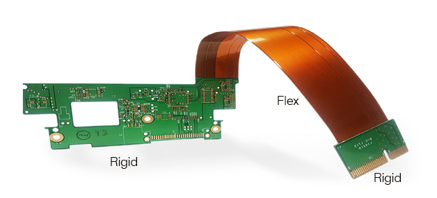
The Definition of Rigid Flex PCB
The Benefit of Rigid Flex PCB
Space Efficiency: Rigid Flex PCB are extremely space efficient because they eliminate the need for connectors and reduce the need for additional interconnections. They can be folded or bent to fit into tight spaces, making them ideal for compact and densely arranged electronic equipment.
Reliability: The fewer connectors there are, the fewer potential points of failure, which increases the reliability of the entire system. Rigid Flex PCB are less prone to connector-related problems.
Durability: Rigid Flex PCB can withstand mechanical stress, vibration and temperature changes, making them suitable for use in harsh environments.
Cost-Effective: Rigid Flex PCB help you minimize overall PCB size, replace board-to-board connectors, and reduce the number of assembly processes. This can lead to significant savings in logistics costs.
Complex Geometries: Rigid flex technology allows for the creation of complex board shapes and three-dimensional configurations that are difficult to achieve with traditional PCBs.
The Capability Overview of Rigid Flex PCB
| Item | Mass Production | Prototype |
| Number of Layers | 2-18 L | 2-20 L |
| Max Board Size | 480*800mm | 480*800mm |
| Outline Dimensional Tolerance | ±0.10mm (≤100mm) ±0.10%mm (>100mm) |
±0.10mm (≤100mm) ±0.10%mm (>100mm) |
| Thickness Range | 0.3-3.2mm | 0.3-4mm |
| Thickness Tolerance (Thk≥0.8mm) | ±8% | ±8% |
| Thickness Tolerance (Thk<0.8mm) | ±10% | ±8% |
| Dielectric Thickness | 0.03-5.00mm | 0.03-5.5mm |
| Minimum Outer Line Width /Line Spacing | 0.075/0.075mm (Finished copper≤1OZ) | 0.075/0.075mm (Finished copper≤1OZ) |
| Min Inner Layer Line Width /Line Spacing | 0.05mm/0.05mm (Base copper 12um) | 0.05mm/0.05mm (Base copper 12um) |
| VIA PAD Min Annular Ring (Double sided) | ≥0.05mm | ≥0.05mm |
| Minimum Distance of Conductor from Outline or NPTH | ≥0.15mm | ≥0.15mm |
| Min Annular Ring (Four Layers and Above) | ≥0.1mm | ≥0.1mm |
| Outer Finished Copper | 35-105um | 35-140um |
| Inner Copper | 12-70um | 12-105um |
| Hole Size (Mechanical Drill) | 0.10-6.35mm | 0.10-6.5mm |
| Laser Drilling (Hole-filling Electroplating is Required) | 0.075-0.1mm | 0.05-0.15mm |
| Aperture Tolerance (mechanical drill) | PTH±0.075mm NPTH±0.05mm | PTH±0.05mm NPTH±0.04mm |
| Hole Position Tolerance (mechanical drill) | ±0.05mm | ±0.05mm |
| Minimum Distance from Inner Hole Edge to other Network Conductor | (4 Layers) 5mil, (6 Layers) 6mil, (8 Layers and above) 8mil |
(4 Layers) 5mil, (6 Layers) 6mil, (8 Layers and above) 8mil |
| Alignment Deviation between Layers (Non-adjacent Layers) | ±0.1mm | ±0.1mm |
| Alignment Deviation between Layers (Adjacent Layers) | ±0.05mm | ±0.05mm |
| Aspect Ratio -Through Hole | 12:1 | 13:1 |
| Aspect Ratio-Blind Hole & Microvia | 2:1 | 2:1 |
| Solder Mask to Position Tolerance (Ink) | ±0.05mm | ±0.038mm |
| Min Soldermask Bridge | 0.1mm | 0.08mm |
| Minimum Distance of PAD without Ink | 0.05mm | 0.04mm |
| Minimum Distance between Ink and Circuit or Copper | 0.05mm | 0.04mm |
| Solder Mask or Silkscreen Color | White/Black/Yellow/Green/Red/Blue/Gray | White/Black/Yellow/Green/Red/Blue/Gray |
| Position Accuracy of Silkscreen | ±0.3mm (semi-automatic) | ±0.2mm (Spray silkscreen) |
| Minimum Line Width of Silkscreen | ≥0.1mm (silkscreen, legend height≥0.8mm) | ≥0.075mm (Spray silkscreen, legend height≥0.65mm) |
| Plug Hole Diameter | 0.1-0.5mm ( Plug hole resin) 0.1-0.25mm (Plug hole ink) |
0.1-0.6mm (Plug hole resin) 0.1-0.3mm (Plug hole ink) |
| Surface Treatment Type | HAL, ENIG, Imm tin, Imm AG, OSP, Planting Gold | HAL, ENIG, Imm tin, Imm AG, OSP, Planting Gold |
| Spacing from The Min Hole Edge to the Cover Opening Area | 0.7mm | 0.6mm |
| Minimum Open Cover Width | 1.5mm | 1.2mm |
| Minimum Distance between Circuit and Cover Opening Area | 0.5mm | 0.4mm |
| Countersunk hole can be machined for Angle and depth tolerances |
Angle: 90°, 120°, 180° Depth Tolerances: +/-0.15mm |
Angle: 90°, 120°, 180° Depth Tolerances: +/-0.13mm |
| Resistance Tolerance | Characteristic Resistance: ±10% Differential Resistance: ±10% |
Characteristic Resistance: ±8% Differential Resistance:±8% |