 Shenzhen Lianjincheng Precision Manufacturing Co., Ltd.

Introduction
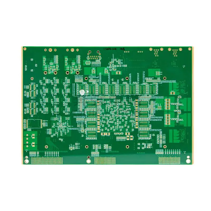
HDI
In modern high-frequency electronic devices, HDI (High Density Interconnector), also known as HDI PCB, serves a pivotal role. Its unique microvia technology and high-density design not only enhance device performance but also propel the evolution of electronic equipment towards smaller, faster, and more reliable form factors. This article delves into the working principle, application scenarios, advantages, and future prospects of HDI circuit boards in high-frequency electronic devices.
Working Principle
The working principle of HDI circuit boards primarily relies on microvia technology and plating techniques. Microvia technology creates tiny vias within insulating materials, which are subsequently filled with conductive materials through plating processes, establishing dense conductive pathways. This design facilitates swift and efficient current flow within devices, boosting signal transmission speed and efficiency. Furthermore, HDI boards incorporate blind and buried via technologies, further enhancing wiring density and reliability.
Application Scenarios

HDI board Application Scenarios
HDI circuit boards find extensive applications in high-frequency electronic devices. In the communications sector, they are prevalent in base stations, routers, switches, and other equipment demanding high signal transmission speeds and reliability. In the computer realm, HDI boards constitute crucial components of motherboards, graphics cards, memory modules, supporting high-speed, reliable data exchanges. Additionally, consumer electronics such as smartphones, tablets, and TVs heavily rely on HDI PCBs to meet their demands for slimness and high performance.
Advantages

Advantages of HDI Circuit Boards
High Density
HDI circuit boards offer higher integration and reduced volumes, enabling the accommodation of more electronic components within limited spaces. This lowers system costs, enhancing system reliability and performance.
High Reliability
Employing advanced manufacturing processes and materials, HDI boards withstand higher voltages and temperatures, mitigating high-frequency noise and electromagnetic interference, thereby improving electronic device stability and reliability.
High Performance
Capable of carrying more signals and currents, HDI circuit boards elevate signal quality and transmission performance, fostering more efficient and reliable electronic device operations.
Development Prospects
HDI circuit board Development Prospects
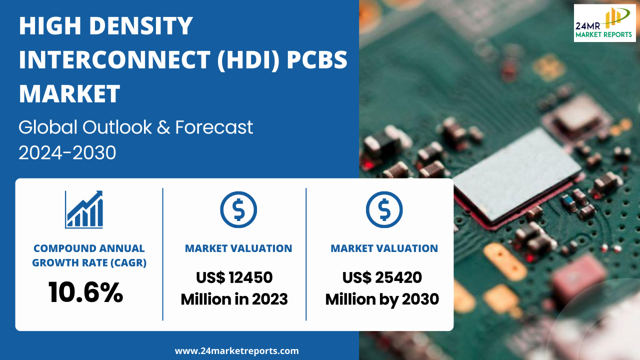
Amidst the escalating global demand for AI computing power, the HDI circuit board market confronts unprecedented growth opportunities. According to authoritative forecasts, the HDI PCB market is projected to reach USD 14.58 billion by 2027, underscoring robust growth potential and vast prospects. Notably, the application demand for HDI circuit boards will persist in high-end smartphones, AI servers, communication equipment, and more. Simultaneously, technological advancements will refine HDI circuit board manufacturing processes, enhancing their performance, and providing sturdier support for electronic device advancements.
Conclusion
As the core driving force in high-frequency electronic devices, HDI circuit boards, with their unique working principles, vast application scenarios, and notable performance advantages, occupy a pivotal position in modern electronics. With continuous technological advancements and growing market demands, HDI circuit boards will permeate every aspect of human life, ushering in an even broader developmental horizon.