 Shenzhen Lianjincheng Precision Manufacturing Co., Ltée.
- Téléphone: +86-18320991841
- E-mail: sales@ljcpcbtech.com
- sales01@ljcpcbtech.com

PCB multicouche
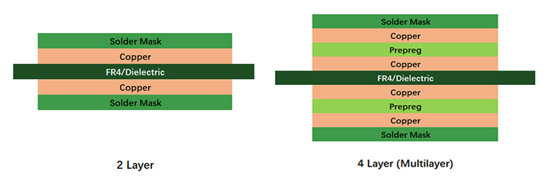
The Definition of Multilayer PCB
Compared with double-sided PCB or a 2-layer PCB board, Multi-Layer or Multilayer Printed Circuit Boards (PCB), or Multilayer Boards (MLBs) must have a minimum of 3 conductive layers of conductive material or copper layer. All the layers are interconnected with copper plated holes, including NC vias and laser micro-vias either in plated through, or in buried and blind.
The Benefit of Multilayer PCB
Multilayer PCB can support a high level of circuit complexity because they consist of three or more copper layers laminated together.
Compact Size: Multilayer PCB reduces the overall size of electronic devices by combining multiple board functions into a single compact board.
Increased Component Density: With internal conductive layers and interlayer vias, multilayer PCB allows more components per unit area, enabling complex circuits to be realized in limited space.
Higher Reliability: Stronger bonds between laminated layers in multilayer PCB provides better resistance to temperature fluctuations, vibration, humidity and mechanical stress.
Improved Electrical Performance: Multilayer PCB provide dedicated signal, power, and ground planes for enhanced noise isolation, controlled impedance routing, and reduced EMI.
Enhanced Heat Dissipation: The planar layers in multilayer PCB can be patterned to efficiently direct heat away from critical areas for improved heat dissipation.
Easy Assembly / Testing: Integrating several simpler boards into a single multilayer PCB simplifies the assembly and testing process.
Design Flexibility: multilayer PCB allows for easier last-minute modifications by rewiring in the inner layers, providing greater flexibility than single or double-layer boards.
The Capability Overview of Multilayer PCB
| Article | Production de masse | Prototype | |
| Layer Count (Max) | 18 | 24 | |
| Board Material | High Frequency, Normal & High Tg FR4, IMS | High Frequency, Normal FR4, IMS, Hybrid Material | |
| Max. Copper Thickness | 6 OZ | 9 OZ | |
| Min. Core Dielectric Thickness | 0.0635 mm | 0.05 mm | |
| Layer to Layer Registration Tolerance | ±0.0635 mm | ±0.05 mm | |
| Épaisseur du panneau fini | 0.4-5.0 mm | 0.35-5.0 mm | |
| Drilled Hole Size-Mechanical | 0.2-7.5 mm | 0.2-8.0 mm | |
| Min. Drilled Hole Size-Laser | 0.075 mm | 0.0635 mm | |
| Min. Buried Hole | 0.15 mm | 0.15 mm | |
| Press Fit Hole Tolerance | ±0.045 mm | ±0.04 mm | |
| Plated Through Hole Tolerance | ±0.0635 mm | ±0.05 mm | |
| Non-Plated Through Hole Tolerance | ±0.038 mm | ±0.025 mm | |
| BGA Pitch (with trace) | 0.45 mm | 0.4 mm | |
| Single-ended /Differential Impedance | ±8% | ±6% | |
| Min. Space Edge to Conductor | 0.175 mm | 0.15 mm | |
| Plating Aspect Ratio | 12:1 | 14:1 | |
| Minimum Line Width/Space (Inner Layer) | 1/2 oz Base Cu | 2.8/ 2.8 mil | 2.5 / 2.8 mil |
| 1 oz Base Cu | 3.2 / 3.8 mil | 3.0 / 3.5 mil | |
| 2 oz Base Cu | 5.2 / 5.6 mil | 4.8 / 5.2 mil | |
| 3 oz Base Cu | 6.5 / 8.0 mil | 6.2 / 7.5 mil | |
| 4 oz Base Cu | 8.6 / 10.2 mil | 8.2 / 9.8 mil | |
| 5 oz Base Cu | 10.0 / 11.5 mil | 9.5 / 11.0 mil | |
| Minimum Line Width/Space (Outer Layer) | 1/3 oz Base Cu | 2.8 / 3.0 mil | 2.5 / 2.8 mil |
| 1/2 oz Base Cu | 3.2 / 3.6 mil | 3.0 / 3.5 mil | |
| 1 oz Base Cu | 5.2 / 5.6 mil | 4.8 / 5.2 mil | |
| 2 oz Base Cu | 7.0 / 7.5 mil | 6.5 / 7.0 mil | |
| 3 oz Base Cu | 9.0 / 10.5 mil | 8.5 / 10.0 mil | |
| 4 oz Base Cu | 11.0 / 12.5 mil | 10.5 / 12.0 mil | |
| Solder Mask Registration | ±0.038 mm | ±0.025 mm | |
| Min. Solder Dam | 0.0635 mm | 0.06 mm | |
| Controlled Depth Drilling Tolerance | ±0.05 mm | ±0.05 mm | |
| Min. Delivery Panel Size | 60×75 mm | 60×60 mm | |
| Max. Delivery Panel Size | 520×600 mm | 520×650 mm | |
| Warpage Control | 0.45% max | 0.4% max | |
| Plated Over Filled Vias(POFV) | YES | YES | |


